
ECE 442 Project Report
Computer System and Memory Design
Sashisu Bajracharya
Sukhonthip Rueangvivatanakij
Team 4
Spring 2002
Dr. D. Tabak
Abstract
The purpose of the project is to design a computing system with instruction sets and memory and cache management. We have to develop the superscalar system with 8-issue instructions per cycle. Further the instruction set is designed for the total of 55 instructions which provides all the general and sufficient programming needs. The instruction set is designed as register-to-register or Load/Store architecture similar to what RISC system has. Our system supports direct, immediate and absolute addressing modes. Moreover, we have branch prediction mechanism of Bimodal Local Branch Prediction which is used for speculative execution to support instruction level parallelism. Moreover, we have Reorder Buffer for reordering the commit of instructions which are executed in parallel. We have Renamed Registers to remove artificial dependence like WAW and WAR data hazards to provide full parallelism. We have multiple functional units as the program generally needs for typical 8 instructions at a time. We also have reservation stations before each execution units in order to keep the instructions until all the input operands are ready. Further, we design the cache and main memory with given specifications. Our cache as specified is set-associative type which has 4 lines (blocks) per set. We implement different cache policies like random replacement, write-through, write-allocate when we build the VHDL model for cache, main memory and CPU. We do the simulation of data transfer between CPU and cache and main memory showing HIT-read, HIT-write, MISS-read and MISS-write. We also do simulation for 8-issue instructions fetching and dispatching to corresponding units.
Specifications
The specifications that are required for the project are:
System and Instruction Set Design
Memory and Cache Management Design
We specified additional design parameters as suitable for our project:
Description of Design
We have,
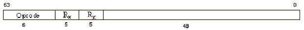
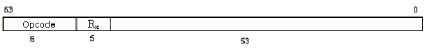
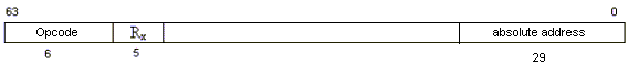
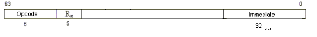
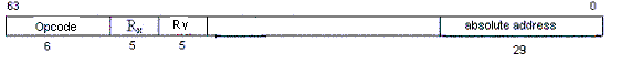
Word Size : 64 bits
Register size: 32 registers. Thus, 5 bits are needed to refer to particular register
Number of instructions: 55 (designed)
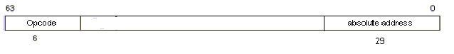
Since, 55 < 64 = 26 , 6 bits are all we need for Opcode.
Memory Size = 512 Mbytes = 229
So, we need 29 bits for absolute memory address
We have chosen immediate operand to have 32 bits.
We chose 3 addressing modes:
1. Register Direct
2. Immediate
3. Absolute
Since other instructions than Load/Store instructions do not access the memory, the instruction operates on register to register, we did not need to put addressing mode bits inside the Instruction. Instead, the opcode carries the information to tell if the instruction involves absolute address or just register or immediate values.
The instruction formats are shown as follows for different types of instructions:
Instruction Format
Word Size : 64 bits
Register : 32 registers à 25 = 5 bits needed to refer Register
No. of instr : 55 < 26 = 6 bits opcode
3-operand Register to Register
2-Operand Register to Register
1-Operand
LOAD/STORE
IMMEDIATE
JUMP
BRANCH ON CONDITION
Our instructions are mainly divided into 4 general groups: Arithmetic type, Logic, Control and Data Transfer type. The list of instructions is as follows:
             Opcodes         Instruction	Operation Performed		Comment
Arithmetic
1)	000000	 ADDF 	Rx, Ry, Rz  ;	Rx =Ry + Rz	 [Floating point Addition]
2)	000001	 SUBF	Rx, Ry, Rz  ;	Rx = Ry - Rz	[Floating point Subtraction]
3)	000010	 MULF   Rx, Ry, Rz  ;	Rx =Ry * Rz	Floating point multiplication
4)	000011	 DIVF 	Rx, Ry, Rz  ;	Rx =Ry / Rz	Floating point Division

5)	000100	 ADD	Rx, Ry, Rz  ;	Rx =Ry + Rz	  [Interger Addition]
6)	000101	 SUB	Rx, Ry, Rz  ;	Rx = Ry - Rz	[Interger Subtraction]
7)	000110	 MUL   	Rx, Ry, Rz  ;	Rx = Ry(32) * Rz(32)	Integer Multiply lower 32 bits of sources
8)	000111	 DIV	Rx, Ry, Rz  ;	Rx = Ry / Rz	Integer Division, Rx gets 	Quotients
9)	001000	 MOD 	Rx, Ry, Rz  ;	Rx = Ry % Rz	Rx  gets remainder of division
10)	001001		DEC     Rx      ;    	Rx  = Rx  - 1 	Decrement by 1
11)	001010		INC     Rx      ;    	Rx  = Rx  + 1 	Increment by 1
12)	001011		CLR	Rx      ;     	Rx  = 0 	Clear the register to 0
13)	001100		NEG    Rx      ;     	Rx  = 0 - Rx 	Change to 2’s Complement
14)	001101		SEW 	Rx                    ;       		Sign Extends 16 bit to 64 bit
15)	001110		SEL 	Rx                    ;      		Sign Extends 32 bit to 64 bit
16)	001111		NOP                      ;		No operation


Logic

17)	010000		AND	Rx, Ry, Rz  ;	Rx = Ry AND Rz 	Logical AND of each bit
18)	010001		OR	Rx, Ry, Rz  ;	Rx  = Ry OR Rz 	Logical OR of each bit
19)	010010		NOT    Rx    ;    	Rx  = 1’s complement of  Rx	bits flipped
20)	010011		XOR 	Rx, Ry, Rz  ;	Rx  = Ry XOR Rz  	Logical XOR of each bit
21)	010100		ROR	Rx       ;     	  	Rotate right with carry
22)	010101		ROL	Rx       ;     	 	Rotate left with carry
23)	010110		SHR	Rx       ;     	 	Shift right Rx with carry
24)	010111		SHL	Rx       ;                	Shift left Rx with carry
25)	011000		SAR	Rx       ;                 	Shift Arithmetic right with							high order bit copied
26)	011001		TST	Rx        ;         		Sets or Clears ‘Z’ & ‘N’ flag
27)	011010		CLC               ;		Clears Carry flag
28)	011011		CLV 	      ;                                       	Clear Overflow flag
29)	011100		SEC           ;		Set Carry Flag
30)	011101		SEV	     ;		Set Overflow Flag

Control Instruction

31)	011110		JMP 	X              ; 	PC =X	Jump to Absolute Address X
32)	011111		BEQ 	Rx, Ry,  X   ;     if Rx -  Ry  = 0, PC=X	If Rx = Ry ,Jump to address X
33)	100000		BNE	Rx, Ry,  X   ;   	if Rx -  Ry  ¹ 0, PC=X	If Rx ¹ Ry ,Jump to address X
34)	100001		BGT 	Rx, Ry,  X   ;     if Rx -  Ry  > 0, PC=X	If Rx > Ry ,Jump to address X
35)	100010		BLT	Rx, Ry,  X   ;     if Rx -  Ry  < 0, PC=X	If Rx < Ry ,Jump to address X
36)	100011		BGE	Rx, Ry,  X   ;     if Rx -  Ry  >= 0, PC=X	If Rx >= Ry ,Jump to address X
37)	100100		BLE 	Rx, Ry,  X   ;     if Rx -  Ry  <= 0, PC=X	If Rx <= Ry ,Jump to address X
38)	100101		JSR	X      ;     	SP = SP - 8, 	Jump to Subroutine with 							(SP) =(PC), PC=X 	address X
39)	100110		RTS                       ;     PC =((SP))       	Return from subroutine
				SP = [SP] + 8
40)	100111		RTI	                  ;	                             Return from Interrupt loads all the Previously saved
						Registers, SP and PC
Data Transfer

41)	101000	PUSH	Rx   ;     	SP =SP - 8,	Push Rx contents to stack
				    (SP) = Rx
42)	101001	POP 	Rx   ;     	Rx  =    (SP),	Pop From stack to Rx
	    	 	       SP = SP + 8
43)	101010	LOAD	Rx , M1 ;   	Rx = M[M1]8	 Load 8 bytes from memory Starting at M1						to Rx
44)	101011	STORE M1, Rx  ;   	M[M1]8 = Rx	 Store 8 bytes to memory starting at M1					     	from Rx
45)	101100	MOVE	 Rx, Ry   ;   	Rx  =  Ry                               	Copy the contents of Ry to Rx
46)	101101	LOADI  Rx , #Im  ;   	Rx  =  #Im	Load Immediate number 	to Rx
47)	101110	EXCHG  Rx , Ry   ;    	(Rx ) <=> (Ry )	Exchange values of Rx  								and Ry
48)	101111	TSR	Rx     ;   	Rx  = SP	Transfer SP address to Rx
49)	110000	TRS 	Rx         ; 	SP = Rx   	Transfer Rx  value to SP
50)	110001	LOADB  Rx , M1    ;   	Rx  = M[M1]1 	Load 1 byte from M at M1 							to Rx
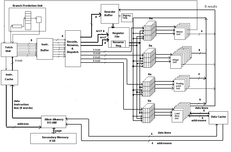
The Fetch Unit, Instruction Buffer, Branch Prediction Unit and Instruction cache is shown in detail as follows:
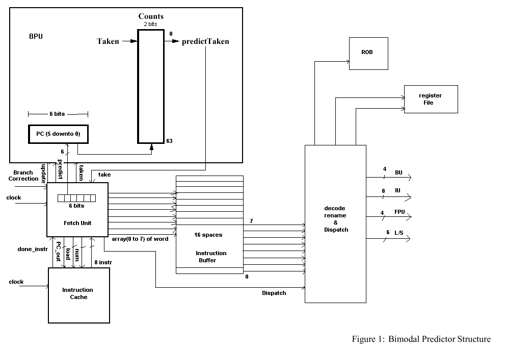
Fetch Unit
The fetch unit provides the first stage of the pipeline and starts the multiple issue instruction level parallelism. In our case it fetches 8 instructions at a time form Instruction Cache starting from address "PC_out" signal to Instruction Cache. In order to fetch the instructions the Fetch Unit puts the first address of the instructions to "PC_out" signal and put the number of instructions that it wants to fetch and sets the ‘load’ to high to notify Instruction cache to transfer the set of instructions. The Instruction Cache returns those set of instructions in "instr" bus which can hold up to 8 instructions. Now the fetch unit checks if any of the instruction is Control(Branch) instruction. If it finds a branch instruction it sends the lower 6 bits of address of that instruction to Branch Prediction Unit (BPU) and set "predict" signal to high to notify the BPU. The BPU will return back the prediction to take or not to take through "take" signal. If the prediction was not to take and all the branch instruction in the set of 8 had been predicted, then the fetch unit issues those set of 8 instructions to the Instruction Buffer. If the prediction is to take, then the instructions of quantity of remaining after that branch instruction in the set of 8 has to be fetched starting from the branch target address. So, once again the remaining new set of instructions is requested to Instruction Cache which will supply that needed number of instructions to the fetch unit. The fetch unit will then transfer the 8 instructions to the Instruction Buffer.
After the set of instructions had been executed, the Branch type instruction will return the information of branch taken or not taken to the Fetch Unit and also to Reorder Buffer. The fetch unit will then send the "update" signal to BPU to modify the corresponding branch prediction entry for the next prediction. It does so by making "update" signal to high and putting address of last 6 bits to "branch_addr" and branch taken or not taken information through "taken" signal.
Also if the branch was mispredicted then new set of instructions are fetched from the Fetch Unit with similar process as before and old set of mispredicted instructions are flushed out from Reorder Buffer and in any Reservation Stations.
Branch Prediction Unit
The branch prediction unit contains 64 entries of two bits which gives the information about the branch to take or not to take. This prediction scheme that we have used is the Bimodal Branch Prediction scheme. The 64 entries are addressed by the last 6 bits of branch instruction. So, each entry correspond to a branch instruction at a particular location in the program. The two bits contents can have 4 possible values: 00, 01, 10, 11.
The unit initiates its action for two situations: one when the "predict" input is high and the other when the "update" input is high. When the "predict" input is high, the corresponding 6 bits of input is read to get the position of entries of the branch in the table. Then prediction is done. The most significant bit determines the prediction. Here, 00 and 01 signifies the prediction of not to take the branch. The 10 and 11 implies the prediction to take the branch. The predicted bit is returned through "take" output to Fetch Unit. If the update bit is high, then the BPU gets to the position located by 6 bit input of "branch_addr" and according to information from "taken" input bit, if the particular branch was actually taken, its corresponding entry is incremented with saturating on 11. If the branch was not actually taken, the corresponding entry is decremented with saturating on 00. Repeatedly taken branch will be predicted to be taken, and repeatedly not-taken branches will be predicted to be not-taken.
Instruction Buffer
The instruction buffer has 16 entries which holds the instructions and sends the first 8 instruction to the Decode, Rename & Dispatch unit. If there is a stall then it temporarily holds the instruction and stores the newly fetched instruction in the last positions.
Decode, Rename & Dispatch Unit
After the set of 8 instructions are issued from the Instruction buffer unit, each instruction is decoded for its opcode in this unit. Depending on the type of instruction to be either Control Instruction, Integer Operation, Floating-point operation or Data transfer operation, the dispatch unit dispatches the instructions to the particular Reservation Stations of corresponding execution units. Since we have decided to have 4 Branch Units(BU), 8 Integer Units(IU), 4 Floating Point Units(FPU) and 6 Load/Store Units(LSU), if in the set of 8 instructions there are instructions greater than the number of Execution Units of particular type, the instructions are queued in the Reservation Stations.
The decode, rename and dispatch unit checks for operands in the Register File and sets the register file to output two or one operands depending on the instruction type to corresponding field in the Reservation Units. While checking for the source and destination operands of the 8 instructions at a time, it checks for any data dependencies between those instructions and previous pipelined instructions including RAW (Read After Write) hazard, WAW (Write after Write) and WAR (Write After Read) hazards. WAW and WAR hazards are removed by assigning the new Rename Register to that particular operand after finding those hazards, puts the mapping of architected register to renamed register in the mapping table and sends the address of that Rename Register to the Reservation Stations through Register File.
Moreover, the instruction gets an entry in the Re-order Buffer in the order of issue. The entry resides there until the instruction gets executed, dependencies resolved, and the instruction committed. When multiple instructions are executed in parallel possibly out-of-order, the result is written in the corresponding entry in the Reorder Buffer of that instruction.
Reorder Buffer
The reorder buffer is the buffer with one entry per active instruction which has been dispatched for execution but not yet committed. This buffer is implemented as a FIFO queue for the active instructions in the order of issue. As instructions are dispatched they are given an entry in the Reorder Buffer. As instructions complete execution in parallel with order instructions which may happen out of order, the result value is placed in the corresponding entry in the Reorder Buffer wherever they are. When the instruction reaches the head of the FIFO buffer, if it has completed execution and dependencies resolved, the entry is removed from the Reorder Buffer and result value placed in the corresponding architected register. The typical Reorder Buffer structure is as follows:
|
Entry |
Busy |
Instruction |
State |
Destination |
Value |
|
1 |
No |
Add R1, R5, R6 |
Commit |
R1 |
11 |
|
2 |
Yes |
Sub R7, R5, R1 |
Write result |
R7 |
|
|
3 |
|||||
|
4 |
Reservation Stations
Reservation Stations (RS) are the temporary storage before the execution units for the instructions that are dispatched and awaiting execution with operands all of which may not be ready at the time of dispatch. The Reservation Station holds the decoded instruction until it is free of all the dependencies and the execution unit is free to execute the instruction. When an instruction is dispatched to the Reservation Station, any already available operand values are read from the register file and placed in the reservation station. After that, the RS checks for the operand names of unavailable data with the result operands of completing instructions that comes back to RS through feedback bus. If there is a match, the result value is placed on the reservation station. When the instructions in RS have all of its operand ready, then the instruction is issued to the execution unit if it is free. There is separate Reservation Stations for each number of individual functional unit to provide the efficient flow of parallelism. The structure of the Reservation Station looks as follows:
|
operation |
source1 |
data1 |
valid1 |
source2 |
data2 |
valid2 |
destination |
The decoded opcode is stored on the operation field. The two source operands are designated in source1 and source2. The data field contains the value of the operands. The valid bit indicates if the data value is present in the reservation station. As an instruction completes and produces result data, a comparison of the instruction’s destination field is compared with the source fields of the instructions in the reservation station. If it matches, the data is written to data field and the valid bit is set. If all the source operands are ready, then the instruction is issued to the execution unit for its execution.
Instruction Execution and Comitting
We have 4 different general types of execution units: Branch Unit, Integer Unit, Floating Point Unit, Load/Store Unit where each have their Reservation Stations to support instruction level parallelism. We have 4 Branch Units, 8 Integer Units, 4 Floating Point Units, 6 Load/Store Units which has been decided on our design considering 8-issue superscalar system and the relative average occurrence of particular type of instructions and the cost considerations. These units execute all the 55 instructions that we have designed for our Instruction Set. Integer Arithmetic, Logic instructions and some data transfer between registers are handled by Integer Unit. Floating Point arithmetic is handled by Floating Point Unit. Control Instructions including Jump and Branch on condition are handled by Branch Unit. Load/ Store Instruction and instructions involving data transfer to memory are handled by Load/Store Unit.
When the execution of instruction is finished, the result operand value is sent to the Reorder Buffer for corresponding entry, sent as feedback to Reservation Stations and also sent to Data Cache if it was a Store type instruction. The Load instruction initiates data transfer from Data Cache and sends the result back to Reorder Buffer. When the result is sent back to all the Reservation Stations, it is compared with all the pending operands that is waiting for the result. If it matches then the result value is written to the corresponding source operand field. This provides the forwarding mechanism to make data available to waiting instruction as soon as possible which reduces instruction stall that might have arisen with the late availability of the data.
When the result value of instruction executed is sent to the Reorder Buffer, the corresponding entry for the instruction gets the destination value. If the destination is the rename register the corresponding rename register in the Register File is updated. If the instruction also reaches the first 8 positions of the FIFO Reorder Buffer, then the result value is updated in the actual architected register corresponding to that rename register shown by the mapping table. This is the commit state of the instruction that happens in order satisfying the sequential order in which the program is written.
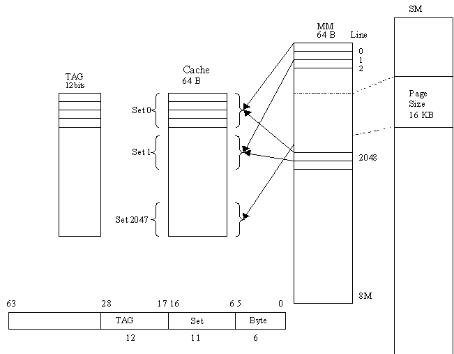
Line (Block) size : 64 Bytes ( 26 B)
Main Memory size : 512Mbytes (229 B)
Number of lines in Memory = 229 / 26 = 223 lines /M
Set = 4 lines/set (22 Lines)
Page size = 16KB (214)
Number of Pages = 229 / 214 = 215 pages/M
Cache size = 512 Kbytes = 219 bytes
Number of lines in Cache = 219 /26 = 213 Lines/cache
Number of sets in Cache = 213/22 = 211 sets/cache
Number of possible lines per one set = ( 223 lines/M) / (211set/cache) = 212 Lines from M can be / set
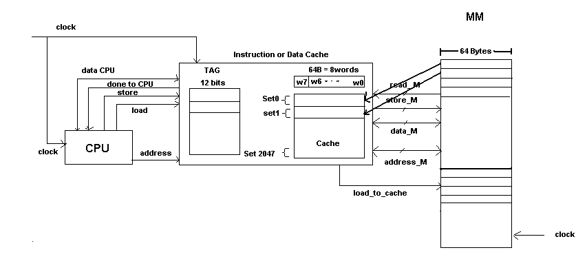
The cache has input and output or bi-directional signals of clock, address, data_CPU, address_M, data_M, load, store, load_to_cache, done_to_CPU, store_M and ready_M. When CPU wants to load a value from memory, it puts the address in address signals of 29 bits and sets the ‘load’ signal to high to notify Cache to load the data. If the CPU wants to store the data to memory, it puts the address in address signals of 29 bits and it sets the ‘store’ signal to high to notify the cache. The cache upon receiving either ‘load’ to high or ‘store’ to high, initiates its action to check if the memory addressed is available in the cache. It went on to steps as shown on the following diagram: 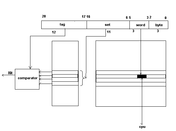
The cache checks ‘set’ number to which the ‘address’ belongs by looking at bits from 16 downto 6 which gives the corresponding set number. Then the cache looks in that set and compares each of the 4 entries’ TAG value with TAG in address(the bits from 28 downto 17). If there is a hit, then corresponding word addressed by bits from 5 downto 3 is accessed. If the instruction was to load(HIT ‘load’), then the corresponding word is returned to the CPU via ‘data_cpu’ signal.
If the instruction was to store on the hit(HIT ‘Store’), then the value of ‘data_CPU is stored in the cache at the corresponding entry. Since we have write-through policy, the corresponding entry in the Main Memory has also to be modified. So, the cache puts the address in the "address_M" signal and data of unit of one "line" (64 Byte) in the "data_M" signal and sets "store_M" to high to notify the main memory. Main memory upon finding "store_M" high stores the line passed in "data_M" signal to the address at "address_M".
However if there is not any match on checking the 4 entries of the set, the "miss" occurs. In this case the main memory has to be accessed. If we have a miss on the ‘load’ instruction by CPU (MISS ‘load’) , then the cache has to fetch that data from the main memory. So, the cache puts the address in the "address_M" and sets its "load_to_cache" signal to high to notify the main memory. Main memory upon receiving this signal, gets the line of data at "address_M" and puts it into the "data_M" signal connected to cache and sets "ready_M" signal to high. The cache upon finding ready_M to high gets the line form "data_M", chooses a random entry, as specified by Random Replacement Policy, in the set and replaces that with the new loaded ‘line’ of data and returns the corresponding word value of 64 bits (denoted by bits 5 downto 3) to CPU through "data_CPU" signal.
If the miss occurs in the ‘store’ instruction by CPU (MISS ‘store’), then since we have decided on our design to have ‘write-allocate’ policy, the missing block(line) from the main memory is loaded going through the same process as in miss in the ‘load’ in previous paragraph. Then it modifies the corresponding word with the new value of "data_CPU" and then its copies back the modified block to the main memory by the same process as in HIT on ‘store’.
However, if the block (line) needed is not even in the main memory, we have the "Page Fault " So page of size 16 Kbyte is loaded from the Secondary Memory to the main memory and the corresponding block is loaded to the cache and then the depending on ‘load’ or ‘store’ instruction the data is either loaded to CPU or stored to cache and the main memory. Writing back to secondary memory occurs only when the page is going to be replaced by another new loading page.
The simulation of memory management and data transfer does the following things:
First the instruction: Load R1, $00000000 is sent by testbench to the CPU where it should create "HIT READ" since the entry is in the cache. The CPU passes the address to cache where it compares the TAG with that of address and returns the data to CPU as it matches. The completion of this instruction takes about 2 clock cycle since only cache access used.
Second the instruction, STORE $00000084, R1 is sent by testbench to CPU where it should result to "HIT WRITE" as the entry is in the Cache initialized before the simulation. However, since the Specification for our design is to have Write-through policy, the cache stores it both to itself and to the main memory. So, the completion of this instruction takes long time about 13 clock cycles since both cache and one memory access are done.
Third the instruction, LOAD R3, $000000a0 is sent by the testbench to CPU where it should result to "MISS READ" since the entry is not put in the cache at the initialization. So when cache checks the TAG it finds the misses to all 4 lines and then requests main memory to transfer the corresponding line to the cache. So, the completion of this instruction takes about 13-14 clock cycles since one memory access is used.
Fourth the instruction, STORE $00000048, R3 is sent by the testbench to CPU where its should create "MISS WRITE" since the entry does not exist during initialization. So when cache checks the TAG in the corresponding set, it finds the miss. Since we decides to use Write-allocate policy, first the corresponding line has to be loaded from memory to cache and then new word value stored at the particular position and then the modified line should be store to memory again. So two memory accesses are used , hence the completion takes about 25 clock cycles as shown on the simulated waveform.
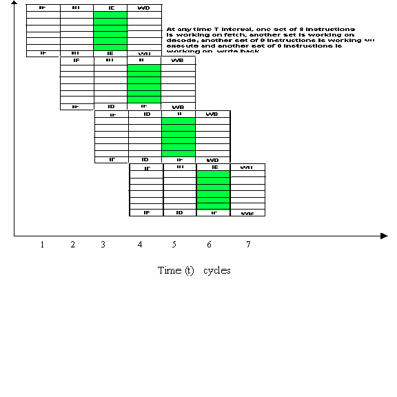
The system was simulated for its fetching unit and decode-dispatch unit in VHDL that shows 8 instructions at a time are being fetched and dispatched to the corresponding unit out of 4 categories of multiple units (BU, IU, FPU, LSU) one after another. This shows the superscaled pipeline of multiple instructions being fetched and dispatched to corresponding execution units. The particular test on VHDL shows three sets of 8 instructions being fetched and issued one after another.
The actual instructions that are used for simulation are:
LOAD R1, $00000000F
ADD R3, R5, R10
Load R09, $00000089
ADDF R20, R18, R24
BEQ R3, R10, $000000A0
shl r4
store $000000B8, r21
load r11, $00000056
-- 1 BU , 3 IU, 1 FPU, 3 LSU instructions in above set of 8
AND R5, R8, R10
SUBF R18, R19, R24
LOAD R31, $00000081
ROR r3
BLE R2, R8, $000000A7
store $00000FFF, r17
MULF R11, R5, R120
BGE R2, R8, $000000A7
-- 2BU , 2 IU, 2 FPU, 2 LSU instructions in above set of 8
ADDF R10, R19, R32
AND R3, R21, R6
SUBF R12, R11, R14
LOAD R31, $00000081
ROL r3
MULF R11, R5, R120
CLR R10
BGE R5, R3, $00000068
-- 1 BU , 3 IU, 3 FPU, 1 LSU instructions in above set of 8
The simulation results are shown in next page:
Overall, the project of System, Instruction Set and Memory and Cache Management design was completed successfully by out team. We learned to design instructions and its format in RISC type instructions which provide full support for Instruction Level Parallelism. The design helped us to explore the workings of superscalar system and purpose of different components like Reorder-Buffer, Reservation Station, Branch Prediction, Rename Registers to provide the performance of Instruction Level Parallelism with multiple issues. We learned the design of memory management and saw the transfer of data between CPU, cache and main memory while simulating our model. In fact, we had the opportunity to implement different cache policies like write-through, write-allocate and random replacement. In turn, the project gave us the design skills and the opportunity to implement various possibilities of building system and memory management.